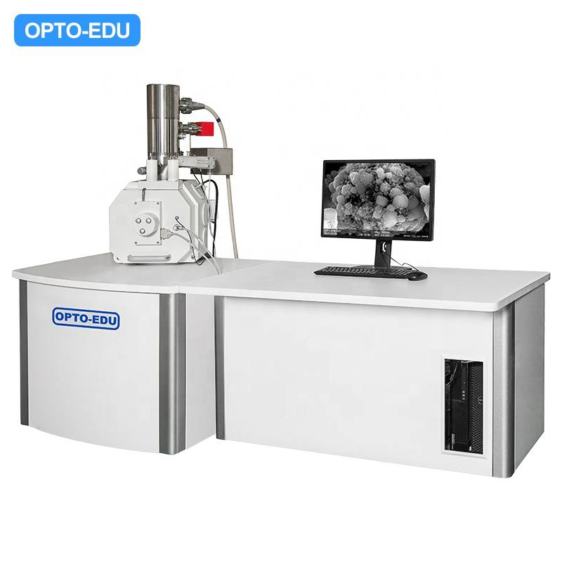
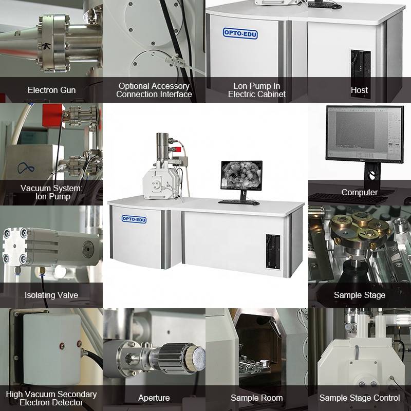
A63.7081 Schottky Field Emission Gun Scanning Electron Mikroskopyo Pro FEG SEM, 15x ~ 800000x


Paghulagway sa Produkto
| A63.7081 Schottky Field Emission Gun Pag-scan sa Elektron nga Mikroskopyo Pro FEG SEM | ||
| Resolusyon | 1nm @ 30KV (SE); 3nm @ 1KV (SE); 2.5nm@30KV (BSE) | |
| Pagpadako | 15x ~ 800000x | |
| Baril sa Elektroniko | Schottky Emission Electron Gun | |
| Kasamtangan nga Electron Beam | 10pA ~ 0.3μA | |
| Nagpadali nga Voatage | 0 ~ 30KV | |
| Sistema sa Vacuum | 2 Ion Pumps, Turbo Molecular Pump, Mechanical Pump | |
| Detector | SE: Taas nga Vacuum Secondary Electron Detector (Nga Adunay Proteksyon sa Detector) | |
| BSE: Upat nga Semiconductor Upat nga Segmentation Balik nga Pagsabwag sa Detector | ||
| CCD | ||
| Yugto sa Sampol | Lima ka Axes Eucentric Motorized Stage | |
| Sakup sa Pagbiyahe | X | 0 ~ 150mm |
| Y | 0 ~ 150mm | |
| Z | 0 ~ 60mm | |
| R | 360º | |
| T | -5º ~ 75º | |
| Max Diameter sa specimen | 320mm | |
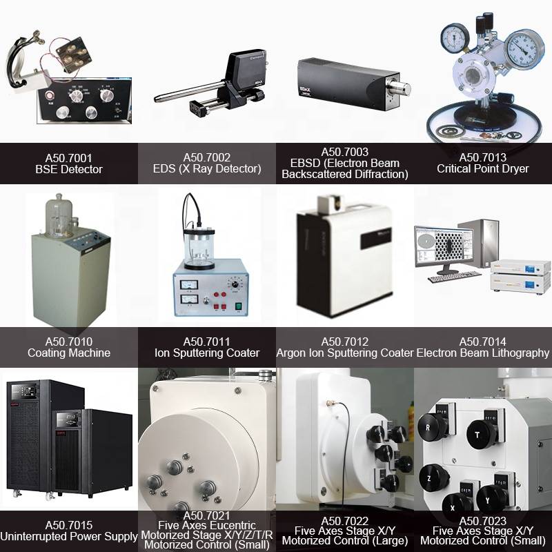
| Pagbag-o | EBL; STM; AFM; Heating Stage; Cryo Stage; Tensile Stage; Micro-nano Manipulator; SEM + Coating Machine; SEM + Laser Etc. | |
| Mga aksesorya | X-Ray Detector (EDS), EBSD, CL, WDS, Coating Machine Ug uban pa | |


Bentaha ug mga Kaso
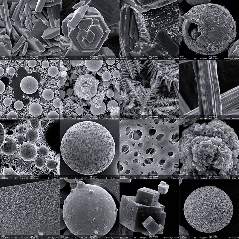
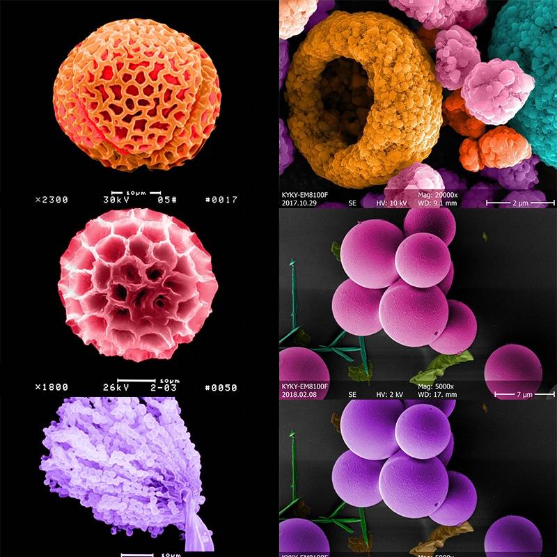
| Ang pag-scan sa electron microscopy (sem) angay alang sa pag-obserbar sa ibabaw nga topograpiya sa metal, ceramics, semiconductors, minerals, biology, polymers, composite ug nano-scale one-dimensional, two-dimensional ug three-dimensional nga mga materyales (ikaduha nga electron image, backscattered electron image). Mahimo kini gamiton aron pag-analisar sa punto, linya ug bahin sa microregion. Kini kaylap nga gigamit sa petrolyo, geolohiya, mineral field, electronics, semiconductor field, medisina, natad sa biology, industriya sa kemikal, polymer material field kriminal nga imbestigasyon sa seguridad sa publiko, agrikultura, kagubatan ug uban pang mga uma. |


Impormasyon sa Kompanya

Isulat ang imong mensahe dinhi ug ipadala kini kanamo